GPUs vs TPUs for Generative AI: Choosing the Right Compute Infrastructure
Training a large language model isn't just about writing clever code. It is a logistics problem. You need massive amounts of memory, lightning-fast data movement between chips, and enough raw calculation power to process trillions of parameters without burning through your entire budget in a week. For years, NVIDIA GPUs were the only game in town. Today, that landscape has shifted. Google’s TPUs have evolved from niche accelerators into serious competitors, especially when you look at cost-per-token and scaling efficiency.
If you are an architect or lead engineer deciding where to run your next foundation model, the choice is no longer obvious. Are you prioritizing ecosystem flexibility with CUDA, or are you chasing the lower total cost of ownership (TCO) that specialized ASICs offer? The answer depends on your team's skills, your cloud provider constraints, and whether you are in the experimental research phase or the production scaling phase.
The Hardware Reality: What Actually Powers LLMs?
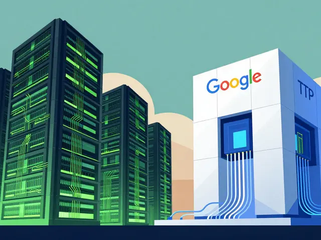
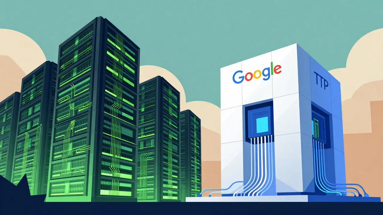
To make a smart decision, you first need to understand what these chips are actually doing under the hood. Both Graphics Processing Units (GPU) and Tensor Processing Units (TPU) are designed for parallel computation, but they approach the problem differently.
NVIDIA H100 GPUs are general-purpose accelerators originally built for graphics rendering. They have been repurposed for deep learning through the CUDA ecosystem. An H100 chip typically delivers around 3,800 tokens per second and comes with 80GB of High Bandwidth Memory (HBM). Newer variants like the H200 extend this memory to 141GB, which is crucial for keeping large models loaded without constant swapping.
In contrast, Google TPU v5p units are Application-Specific Integrated Circuits (ASICs). They are built exclusively for tensor operations-the math behind neural networks. A single TPU v5p chip targets approximately 3,672 TFLOPS. While the raw throughput per chip might look slightly lower than top-tier GPUs on paper, the architecture is optimized for deterministic execution. This means less time waiting for data and more time calculating. In real-world testing, TPU v5p achieves a Model FLOPs Utilization (MFU) of roughly 58%, compared to about 52% for H100s on identical workloads. That 6% difference sounds small, but at scale, it translates to significant speed gains.
| Feature | NVIDIA H100 | Google TPU v5p (8-chip slice) |
|---|---|---|
| Architecture Type | General Purpose GPU | ASIC (Tensor Specific) |
| Memory per Chip | 80 GB HBM | 95 GB HBM (approx. 760 GB total in 8-chip config) |
| Tokens Per Second (Approx.) | 3,800 | 3,450 |
| Model FLOPs Utilization (MFU) | ~52% | ~58% |
| Primary Interconnect | NVLink / InfiniBand | Optical Circuit Switch (OCS) |
The Cost Equation: Why TPUs Are Gaining Ground
Performance metrics matter, but CFOs care about dollars. This is where the conversation changes dramatically. When you break down the hourly costs, the economics start to favor specialized hardware for specific workloads.
An 8-chip node of NVIDIA H100 GPUs typically costs between $12.00 and $15.00 per hour, depending on whether you use Spot instances or Reserved pricing. A comparable slice of eight TPU v5p chips runs between $8.00 and $11.00 per hour. On the surface, that’s a 20-30% savings. But the real advantage comes from availability and scaling.
Google Cloud offers Spot TPUs at up to 70% cheaper rates than on-demand pricing. More importantly, finding large, contiguous blocks of TPUs is often easier than securing massive clusters of H100s, which are frequently oversubscribed due to high demand across all cloud providers. Reports from infrastructure analysts suggest that for pure Large Language Model (LLM) training, TPUs can deliver 4 to 10 times higher cost-effectiveness than GPUs. Even if you don’t hit the extreme end of that range, a performance-per-dollar ratio that is 1.2 to 1.7 times superior makes a compelling case for migration.
The latest generation, TPU v6e, pushes this further, claiming up to four times better performance per dollar compared to the H100 for training and inference tasks. If your primary goal is to train a trillion-parameter model as cheaply as possible, the TPU path currently holds the financial edge.

Distributed Training: How Chips Talk to Each Other
You rarely train a modern foundation model on a single chip. You need thousands of them working together. This is where the architectural differences become critical. Distributed training requires moving gradients and weights between devices constantly. If that communication is slow, your expensive compute cores sit idle, waiting for data.
On the NVIDIA side, the industry standard is NCCL (NVIDIA Collective Communications Library), often used with PyTorch’s torch.distributed. It works well, but it relies on external networking infrastructure like InfiniBand or Ethernet. As clusters grow larger, network congestion and latency can become bottlenecks. You have to manually manage sharding logic and ensure your network topology supports the traffic load.
Google takes a different approach with TPUs. They use the GSPMD compiler, part of the XLA ecosystem. This allows developers to write code for a single device, and the compiler automatically handles how data is split (sharded) across the entire TPU Pod. This removes a huge layer of engineering complexity.
Furthermore, TPU Pods connect via Optical Circuit Switch (OCS) interconnects. Unlike traditional electrical switches, OCS provides superior bandwidth and nearly linear scalability. You can scale up to 4,096 chips in a pod without the performance degradation you often see in GPU clusters. For organizations building next-generation foundation models, this near-linear scaling is a massive technical advantage.
Ecosystem and Developer Experience: The CUDA Moat
If TPUs are cheaper and scale better, why does everyone still use NVIDIA? The answer is ecosystem maturity. CUDA has been the dominant platform for over a decade. It has a massive community, extensive debugging tools, and native integration with popular frameworks like PyTorch.
If you are a researcher experimenting with new architectures, you want to move fast. You want to tweak a custom kernel, debug a weird loss spike, and deploy to multiple clouds without changing your backend code. GPUs excel here. They support eager mode in PyTorch, which makes debugging intuitive. You can prototype quickly, test non-standard layers, and rely on a vast library of pre-built solutions.
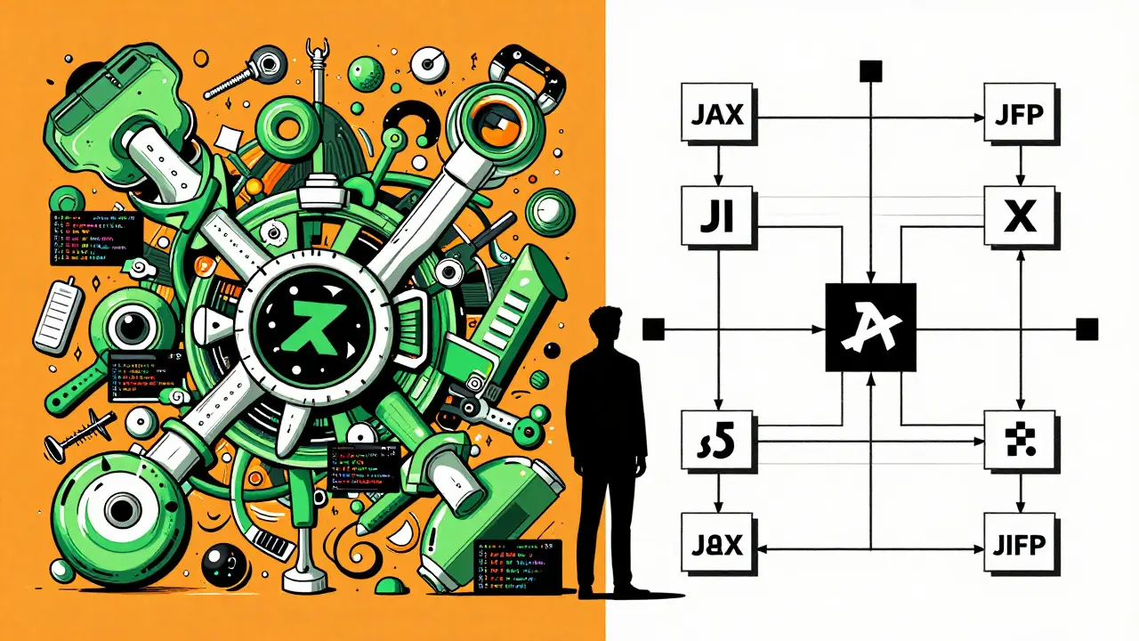
TPUs require you to embrace the XLA ecosystem, primarily using TensorFlow or JAX. While JAX has gained popularity among researchers, the learning curve is steeper. If your model uses custom operations that aren’t supported by XLA, you might hit a wall. Additionally, TPUs are exclusive to Google Cloud Platform (GCP). If your organization has a multi-cloud mandate requiring deployment on AWS or Azure, TPUs add a layer of complexity that GPUs do not.
So, the trade-off is clear: GPUs offer flexibility, portability, and ease of use. TPUs offer efficiency, cost savings, and seamless scaling-but only if you stay within their ecosystem.
Decision Framework: Which One Should You Choose?
There is no single "best" chip. The right choice depends on your specific job-to-be-done. Here is a practical guide to help you decide:
- Choose NVIDIA H100/H200 if:
- You are in the early research or prototyping phase and need rapid iteration.
- Your team is already proficient with PyTorch and CUDA kernels.
- You require multi-cloud portability (AWS, Azure, GCP).
- You are fine-tuning smaller models on single nodes where setup complexity matters more than raw cost.
- You have custom layers or operations not yet supported by XLA.
- Choose Google TPU v5p/v6e if:
- You are pre-training large foundation models (billions to trillions of parameters).
- Cost-per-token is a primary KPI for your project.
- You are willing to adopt JAX or TensorFlow and optimize for XLA.
- You need to scale to thousands of chips with minimal network overhead.
- You are running high-volume inference for millions of users and want to maximize throughput per dollar.
Many sophisticated organizations are adopting a hybrid strategy. They might use TPUs for the heavy lifting of pre-training a base model because of the cost advantages, then switch to GPU clusters for fine-tuning and inference to leverage broader ecosystem tools and multi-cloud distribution. This approach balances the economic benefits of ASICs with the flexibility of general-purpose GPUs.
Future Outlook: The Race Continues
As we move through 2026, the gap between these platforms is narrowing in terms of raw capability, but diverging in terms of strategic positioning. Google is doubling down on TPU investment, training its flagship Gemini models on its own silicon and securing deals with major players like Anthropic. NVIDIA continues to innovate with architectures like the GB300 NVL72, aiming to improve memory density and interconnect speeds to counter TPU’s efficiency gains.
For most teams, the decision will come down to organizational fit. Do you have the engineering capacity to optimize for TPUs? Can you afford the premium for CUDA’s convenience? There is no wrong answer, but there are expensive mistakes. By understanding the true cost of ownership, the realities of distributed training, and the limitations of each ecosystem, you can build an infrastructure that supports your AI ambitions without breaking the bank.
Are TPUs only available on Google Cloud?
Yes, currently TPUs are exclusive to Google Cloud Platform (GCP). If your organization requires a multi-cloud strategy involving AWS or Azure, you will likely need to maintain GPU infrastructure alongside any TPU usage, or stick entirely to GPUs for portability.
Can I use PyTorch with TPUs?
PyTorch has improved support for TPUs through torch_xla, but the experience is not as seamless as it is with JAX or TensorFlow. For best performance and easiest debugging on TPUs, JAX is generally recommended by the community and Google.
What is Model FLOPs Utilization (MFU)?
MFU measures how much of the theoretical peak performance of a chip is actually being used during training. A higher MFU means less wasted compute. TPUs often achieve higher MFU (around 58%) compared to GPUs (around 52%) due to their deterministic execution and efficient interconnects.
Is it worth switching from GPUs to TPUs for fine-tuning?
For small-scale fine-tuning on single nodes, GPUs are often preferred due to lower setup complexity and better tooling support. TPUs shine in large-scale pre-training or high-volume inference. Unless you are fine-tuning very large models across many chips, the cost savings of TPUs may not offset the engineering effort required to migrate.
How does the Optical Circuit Switch (OCS) benefit TPU pods?
OCS connects TPU chips using light instead of electricity, providing higher bandwidth and lower latency. This allows TPU pods to scale to thousands of chips with nearly linear performance growth, avoiding the network congestion issues common in large GPU clusters.